I have “coded” quite some LabVIEW programs over time and I am a member of the Würzburg LabVIEW User Group. Here comes a small selection of programs.
Probably the smallest LabVIEW User Group logo in the word. We have quite an active LabVIEW community here in Würzburg (thanks to Jörg Hampel) and I fabricated this logo for a “Xmas special” where I showed a fraction of the group our clean room and the optical labs (together with Daniel). The logo is carved into a Silicon wafer using a Focused Ion Beam (FIB), the golden piece with the “+” is an actual gold flake and the brownish diagonal line underneath is hair of mine. Human hair typically has diameters around ~50µm.
FlakeFit
FlakeFit is the first LabVIEW program I wrote in order to measure the thickness of Gold flakes using just an optical transmission microscope. It worked astonishingly well with a precision of ~2 nm for flake thicknesses below 100 nm (above not much light is transmitted through the gold anymore) and, nowadays, it is still a working horse in our group. More details can be found in this publication.
The “FlakeFit” LabVIEW program successfully live-fits a model to the transmission spectrum of a Gold flake. Here, it determines a thickness of 31 nm which is accurate within +/- 2 nm. On the right-hand side an Olympus IX70 microscope is depicted on which the sample with the flake is mounted and the transmission measured using an Ocean Optics USB2000 fiber spectrometer.
PlasmoCam
My second program — PlasmoCam — was already much more complex. It was needed for our Electrically-Driven Optical Antenna paper as we applied voltages and wanted to measure the electrical currents and the resulting photon fluxes simultaneously. We used a Keithley sourcemeter to apply the voltages and measure the small currents (pA to nA) and furthermore purchased an Andor EMCCD to acquire images/spectra quickly enough.
PlasmoCam in combined (synchronized) mode with the cyclic IV-tab opened on the left and the spectrum tab on the right-hand side. The white curve is an emission spectrum which is already quantum efficiency corrected, i.e., we can directly see how much light is emitted during the measurement.
PlamoCam initializes and talks to the devices, coordinates the measurements, displays the results, calculates the quantum efficiency corrected spectra in real time, let you browse through the results and of course save them.
PlasmoCam again in combined mode but this time with the I(t) tab opened on the left and the Image tab on the right. The bigger blue shape is a white-light transmission image acquired for orientation purposes and the small spot in the center is the actual light emission of an antenna 274s after the start of the measurement. On the left-hand side on can see the corresponding current (red), voltage (blue) and photon count (white) over. The vertical white line at 274s can be moved to look how the image/spectra looked at different times.
I took me three months to program a first working version which was then used for our publication. As we are still working on nano-electro-optic devices I refactored/rewrote it three times over the years and thanks to the WUELUG it has now a much more modular and robust architecture.
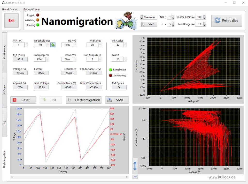
Nanomigration
One of the benefits of the modular design is that it is easy to adapt to new devices (e.g., SuperK continuum laser + AOTF) or to new functions like 2D IV-V scans or electromigrating small gaps into single-crystalline gold structures. (Hint: It doesn’t work like expected.) For the “Nanomigration” program the Oscilloscope, IV-Curve and I(t) modules as well as the whole device interaction logic with the Keithley could simply be reused and only the electromigration logic needed to be implemented within a dedicated module.
The Nanomigration program in action. In the top-right diagram one can see how the resistance increases with each cycle hinting to an ever-decreasing constriction between the positive and negative electrode. The same data is show again in I(t)/V(t) graphs (bottom left) and conductance vs voltage plots (bottom right) to help with the process. Because forming nanogaps is a kind of magic.